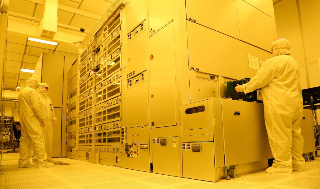
Clean-room technicians at the AIM Photonics NanoTech chip fabrication facility in Albany, New York. Credit: SUNY Polytechnic Institute
Topics: Computer Science, Electrical Engineering, Materials Science, Nanotechnology, Semiconductor Technology
Over 50 Years of Moore’s Law – Intel
GAITHERSBURG, Md. — The U.S. Department of Commerce’s National Institute of Standards and Technology (NIST) has entered into a cooperative research and development agreement with AIM Photonics that will give chip developers a critical new tool for designing faster chips that use both optical and electrical signals to transmit information. Called integrated photonic circuits, these chips are key components in fiber-optic networks and high-performance computing facilities. They are used in laser-guided missiles, medical sensors, and other advanced technologies.
AIM Photonics, a Manufacturing USA institute, is a public-private partnership that accelerates the commercialization of new technologies for manufacturing photonic chips. The New York-based institute provides small and medium-sized businesses, academics, and government researchers access to expertise and fabrication facilities during all phases of the photonics development cycle, from design to fabrication and packaging.
NIST and AIM Photonics Team Up on High-Frequency Optical/Electronic Chips
